

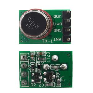
315/433/868/915 MHz RF Transceiver Module
-
Payment


-
Origin
China Mainland
-
Minimum Order
5
-
Packing
Pieces
- Contact Now Start Order
- Description
Product Detail
315/433/868/915 MHz RF Transceiver Module
1. 315/433/868/915 MHz RF Transceiver Module Description
The RY1276 RF transceivers module feature the LoRaTM long range modem that provides ultra-long range spread spectrum communication and high interference immunity whilst minimising current consumption.
Using Semtech’s patented LoRaTM modulation technique SX1276 can achieve a sensitivity of over -148dBm using a low cost crystal and bill of materials. The high sensitivity combined with the integrated +20 dBm power amplifier yields industry leading link budget making it optimal for any application requiring range or robustness. LoRaTM also provides significant advantages in both blocking and selectivity over conventional modulation techniques, solving the traditional design compromise between range, interference immunity and energy consumption.
These devices also support high performance (G)FSK modes for systems including WMBus, IEEE802.15.4g. The SX1276 deliver exceptional phase noise, selectivity, receiver linearity and IIP3 for significantly lower current consumption than competing devices.
2. Applications of 315/433/868/915 MHz RF Transceiver Module
* Automated Meter Reading.
* Home and Building Automation.
* Wireless Alarm and Security Systems.
* Industrial Monitoring and Control
* Long range Irrigation Systems
3. Features of 315/433/868/915 MHz RF Transceiver Module
* LoRaTM Modem
* 168 dB maximum link budget
* +20 dBm - 100 mW constant RF output vs. V supply
* +14 dBm high efficiency PA
* Programmable bit rate up to 300 kbps
* High sensitivity: down to -148 dBm
* Bullet-proof front end: IIP3 = -11 dBm
* Excellent blocking immunity
* Low RX current of 9.9 mA, 200 nA register retention
* Fully integrated synthesizer with a resolution of 61 Hz
* FSK, GFSK, MSK, GMSK, LoRaTMand OOK modulation
* Built-in bit synchronizer for clock recovery
* Preamble detection
* 127 dB Dynamic Range RSSI
* Automatic RF Sense and CAD with ultra-fast AFCf
* Packet engine up to 256 bytes with CRC
* Built-in temperature sensor and low battery retention
4. Pin Diagram of 315/433/868/915 MHz RF Transceiver Module
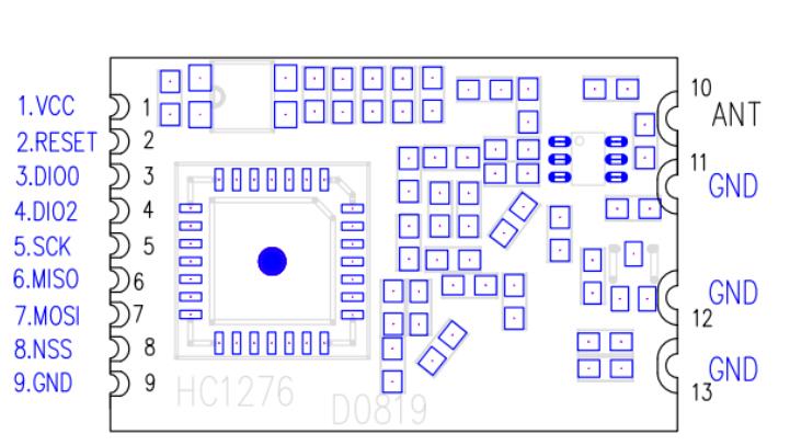
5. Pin Description of 315/433/868/915 MHz RF Transceiver Module
Number | Name | Type | D |
1 | VCC | I | Supply voltage for moudule. |
2 | RESET | I | Reset trigger input. |
3 | DIO0 | I/O | Digital I/O, software configured. |
4 | DIO2 | I/O | Digital I/O, software configured. |
5 | SCK | I | SPI Clock input. |
6 | MISO | O | SPI Data output. |
7 | MOSI | I | SPI Data input. |
8 | NSS | I | SPI Chip select input |
9,11-13 | GND | I | Ground. |
10 | ANT | 0 | RF Output |
6. Electrical Characteristics of 315/433/868/915 MHz RF Transceiver Module
6.1. ESD Notice
The RY1276 is a high performance radio frequency device. It satisfies:
* Class 2 of the JEDEC standard JESD22-A114-B (Human Body Model) on all pins.
* Class III of the JEDEC standard JESD22-C101C (Charged Device Model) on all pins
It should thus be handled with all the necessary ESD precautions to avoid any permanent damage.
6.2. Absolute Maximum Ratings
Stresses above the values listed below may cause permanent device failure. Exposure to absolute maximum ratings for extended periods may affect device reliability.
Table 3 Absolute Maximum Ratings
Symbol |
Description |
Min |
Max |
Unit |
VDDmr |
Supply Voltage |
-0.5 |
3.9 |
V |
Tmr |
Temperature |
-55 |
+115 |
° C |
Tj |
Junction temperature |
- |
+125 |
° C |
Pmr |
RF Input Level |
- |
+10 |
dBm |
Note Specific ratings apply to +20 dBm operation (see Section 5.4.3).
6.3. Operating Range
Table 1 Operating Range
Symbol |
Description |
Min |
Max |
Unit |
VDDop |
Supply voltage |
1.8 |
3.7 |
V |
Top |
Operational temperature range |
-40 |
+85 |
°C |
Clop |
Load capacitance on digital ports |
- |
25 |
pF |
ML |
RF Input Level |
- |
+10 |
dBm |
Note A specific supply voltage range applies to +20 dBm operation (see Section 5.4.3).
7. Power Consumption of 315/433/868/915 MHz RF Transceiver Module
Table 3 Power Consumption Specification
Symbol |
Description |
Conditions |
Min |
Typ |
Max |
Unit | |
IDDSL |
Supply current in Sleep mode |
- |
0.2 |
1 |
uA | ||
IDDIDLE |
Supply current in Idle mode |
RC oscillator enabled |
- |
1.5 |
- |
uA | |
IDDST |
Supply current in Standby mode |
Crystal oscillator enabled |
- |
1.6 |
1.8 |
mA | |
IDDFS |
Supply current in
Synthesizer mode |
FSRx |
- |
5.8 |
- |
mA | |
IDDR |
Supply current in Receive mode |
LnaBoost Off, band 1
LnaBoost On, band 1 |
-
- |
10.8
11.5 |
-
- |
mA | |
IDDT |
Supply current in Transmit mode with impedance |
RFOP = +20 dBm, on PA_BOOST RFOP = +17 dBm, on PA_BOOST RFOP = +13 dBm, on RFO_LF/HF pin RFOP = + 7 dBm, on |
-
-
- |
120
87
29 |
-
-
- |
m
A | |
8. Frequency Synthesis of 315/433/868/915 MHz RF Transceiver Module
Table 4 Frequency Synthesizer Specification
Symbol |
Description |
Conditions |
Min |
Typ |
Max |
Unit |
FR |
Synthesizer frequency range |
Band 1
Programmable Band 2 |
137
410 |
-
- |
175
525 |
MHz |
FXOSC |
Crystal oscillator frequency |
- |
32 |
- |
MHz | |
TS_OSC |
Crystal oscillator wake-up time |
- |
250 |
- |
us | |
TS_FS |
Frequency synthesizer wake-up time to PllLock |
From Standby mode |
- |
60 |
- |
us |
TS_HOP |
Frequency synthesizer hop time
at most 10 kHz away from the tar- get frequency |
200 kHz step
1 MHz step
5 MHz step
7 MHz step
12 MHz step |
-
-
-
-
- |
20
20
50
50
50 |
-
-
-
-
- |
us us us us us |
FSTEP |
Frequency synthesizer step |
FSTEP = FXOSC/219 |
- |
61.0 |
- |
Hz |
FRC |
RC Oscillator frequency |
After calibration |
- |
62.5 |
- |
kHz |
BRF |
Bit rate, FSK |
Programmable values (1) |
1.2 |
- |
300 |
kbps |
BRA |
Bit rate Accuracy, FSK |
ABS(wanted BR - available BR) |
- |
- |
250 |
ppm |
BRO |
Bit rate, OOK |
Programmable |
1.2 |
- |
32.768 |
kbps |
BR_L |
Bit rate, LoRa Mode |
From SF6, BW=500kHz to
SF12, BW=7.8kHz |
0.018 |
- |
37.5 |
kbps |
FDA |
Frequency deviation, FSK (1) |
Programmable
FDA + BRF/2 =< 250 kHz |
0.6 |
- |
200 |
kHz |
Note For Maximum Bit rate the maximum modulation index is 0.5.
9. FSK/OOK Mode Receiver
All receiver tests are performed with RxBw = 10 kHz (Single Side Bandwidth) as programmed in RegRxBw, receiving a PN15 sequence. Sensitivities are reported for a 0.1% BER (with Bit Synchronizer enabled), unless otherwise specified. Blocking tests are performed with an unmodulated interferer. The wanted signal power for the Blocking Immunity, ACR, IIP2, IIP3 and AMR tests is set 3 dB above the receiver sensitivity level.
Table5 FSK/OOK Receiver Specification
Symbol |
Description |
Conditions |
Min |
Typ |
Max |
Unit |
RFS_F_LF |
Direct tie of RFI and RFO pins, shared Rx, Tx paths FSK sensitiv- ity, highest LNA gain. Bands 2&3 |
FDA = 5 kHz, BR = 1.2 kb/s FDA = 5 kHz, BR = 4.8 kb/s FDA = 40 kHz, BR = 38.4 kb/s* FDA = 20 kHz, BR = 38.4 kb/s** |
-
-
-
- |
-121
-117
-107
-108 |
-
-
-
- |
dBm dBm dBm dBm |
Split RF paths, the RF switch insertion loss is not accounted for. Bands 2&3 | FDA = 5 kHz, BR = 1.2 kb/s FDA = 5 kHz, BR = 4.8 kb/s FDA = 40 kHz, BR = 38.4 kb/s* FDA = 20 kHz, BR = 38.4 kb/s** |
-
-
-
- |
-123
-119
-109
-110 |
-
-
-
- | dBm dBm dBm dBm | |
RFS_F_HF |
Direct tie of RFI and RFO pins, shared Rx, Tx paths FSK sensitiv- ity, highest LNA gain. Band 1 | FDA = 5 kHz, BR = 1.2 kb/s FDA = 5 kHz, BR = 4.8 kb/s FDA = 40 kHz, BR = 38.4 kb/s* FDA = 20 kHz, BR = 38.4 kb/s** |
-
-
-
- |
-119
-115
-105
-105 |
-
-
-
- | dBm dBm dBm dBm |
Split RF paths, LnaBoost is turned on, the RF switch insertion loss is not accounted for. Band 1 |
FDA = 5 kHz, BR = 1.2 kb/s FDA = 5 kHz, BR = 4.8 kb/s FDA = 40 kHz, BR = 38.4 kb/s* FDA = 20 kHz, BR = 38.4 kb/s** |
-
-
-
- |
-123
-119
-109
-109 |
-
-
-
- |
dBm dBm dBm dBm | |
RFS_O | OOK sensitivity, highest LNA gain shared Rx, Tx paths |
BR = 4.8 kb/s
BR = 32 kb/s |
-
- |
-117
-108 |
-
- | dBm dBm |
CCR |
Co-Channel Rejection, FSK |
- |
-9 |
- |
dB | |
ACR |
Adjacent Channel Rejection | FDA = 5 kHz, BR=4.8kb/s
Offset = +/- 25 kHz or +/- 50kHz
Band 3
Band 2
Band 1 |
-
-
- |
60
56
50 |
-
-
- |
dB dB dB |
BI_HF |
Blocking Immunity, Band 1 | Offset = +/- 1 MHz Offset = +/- 2 MHz Offset = +/- 10 MHz |
-
-
- |
71
76
84 |
-
-
- | dB dB dB |
BI_LF |
Blocking Immunity, Bands 2&3 | Offset = +/- 1 MHz Offset = +/- 2 MHz Offset = +/- 10 MHz |
-
-
- |
71
72
78 |
-
-
- |
dB
dB
dB |
IIP2 |
2nd order Input Intercept Point
Unwanted tones are 20 MHz |
Highest LNA gain |
- |
+55 |
- |
dBm |
IIP3_HF |
3rd order Input Intercept point
Unwanted tones are 1MHz and
1.995 MHz above the LO |
Band 1
Highest LNA gain G1
LNA gain G2, 5dB sensitivity hit |
-
- |
-11
-6 |
-
- |
dBm dBm |
IIP3_LF |
3rd order Input Intercept point
Unwanted tones are 1MHz and
1.995 MHz above the LO |
Band 2
Highest LNA gain G1
LNA gain G2, 2.5dB sensitivity hit |
-
- |
-22
-15 |
-
- |
dBm dBm |
Band 3
Highest LNA gain G1
LNA gain G2, 2.5dB sensitivity hit |
-
- |
-15
-11 |
-
- |
dBm dBm | ||
BW_SSB |
Single Side channel filter BW |
Programmable |
2.7 |
- |
250 |
kHz |
IMR |
Image Rejection |
Wanted signal 3dB over sensitivity
BER=0.1% |
- |
50 |
- |
dB |
IMA |
Image Attenuation |
- |
57 |
- |
dB | |
DR_RSSI |
RSSI Dynamic Range |
AGC enabled Min
Max |
-
- |
-127
0 |
-
- |
dBm dBm |
* RxBw = 83 kHz (Single Side Bandwidth)
** RxBw = 50 kHz (Single Side Bandwidth)
*** RxBw = 250 kHz (Single Side Bandwidth)
10. FSK/OOK Mode Transmitter
Table 6 Transmitter Specification
Symbol |
Description |
Conditions |
Min |
Typ |
Max |
Unit |
RF_OP |
RF output power in 50 ohms
on RFO pin (High efficiency PA). |
Programmable with steps
Max
Min |
-
- |
+14
-1 |
-
- |
dBm dBm |
?RF_ OP_V |
RF output power stability on RFO
pin versus voltage supply. | VDD = 2.5 V to 3.3 V VDD = 1.8 V to 3.7 V |
-
- |
3
8 |
-
- |
dB
dB |
RF_OPH |
RF output power in 50 ohms, on
PA_BOOST pin (Regulated PA). |
Programmable with 1dB steps Max
Min |
-
- |
+17
+2 |
-
- | dBm dBm |
RF_OPH_ MAX |
Max RF output power, on
PA_BOOST pin |
High power mode |
- |
+20 |
- |
dBm |
?RF_ OPH_V |
RF output power stability on PA_- BOOST pin versus voltage supply. |
VDD = 2.4 V to 3.7 V |
- |
+/-1 |
- |
dB |
?RF_T |
RF output power stability versus |
From T = -40 °C to +85 °C |
- |
+/-1 |
- |
dB |
PHN |
Transmitter Phase Noise |
169 MHz, Band 3
10kHz Offset
50kHz Offset
400kHz Offset |
-
-
- |
-118
-118
-128 |
-
-
- |
dBc
/ Hz |
433 MHz, Band 2
10kHz Offset
50kHz Offset
400kHz Offset |
-
-
-
- |
-110
-110
-122
-129 |
-
-
-
- |
dBc
/ Hz | ||
868/915 MHz, Band 1
10kHz Offset
50kHz Offset
400kHz Offset
1MHz Offset |
-
-
-
- |
-103
-103
-115
-122 |
-
-
-
- |
dBc
/ Hz | ||
ACP | Transmitter adjacent channel power (measured at 25 kHz offset) | BT=1. Measurement conditions as defined by EN 300 220-1 V2.3.1 |
- |
- |
-37 |
dBm |
TS_TR | Transmitter wake up time, to the first rising edge of DCLK | Frequency Synthesizer enabled, PaR- amp = 10us, BR = 4.8 kb/s |
- |
120 |
- |
us |
11. Electrical Specification for LoRaTM Modulation
The table below gives the electrical specifications for the transceiver operating with LoRaTM modulation. Following conditions apply unless otherwise specified:
* Supply voltage = 3.3 V
* Temperature = 25° C
* fXOSC = 32 MHz
* bandwidth (BW) = 125 kHz
* Spreading Factor (SF) = 12
* Error Correction Code (EC) = 4/6
* Packet Error Rate (PER)= 1%
* CRC on payload enabled
* Output power = 13 dBm in transmission
* Payload length = 64 bytes
* Preamble Length = 12 symbols (programmed register PreambleLength=8)
* With matched impedances
Table 7 LoRa Receiver Specification
Symbol |
Description |
Conditions |
Mi |
Typ |
Max |
Unit |
IDDR_L |
TM
mode, LnaBoost off | Bands 2&3, BW=7.8 to 62.5 kHz
Bands 2&3, BW = 125 kHz
Bands 2&3, BW = 250 kHz | -
-
- | 11.0
11.5
12.4 | -
-
- | mA
mA
mA |
Band 1, BW=7.8 to 62.5 kHz Band 1, BW = 125 kHz Band 1, BW = 250 kHz | -
-
- | 9.9
10.3
11.1 | -
-
- | mA mA mA | ||
IDDT_L |
Supply current in transmitter mode | RFOP = 13 dBm
RFOP = 7 dBm | -
- | 28
20 | -
- | mA
mA |
IDDT_H_L | Supply current in transmitter mode with an external impedance |
Using PA_BOOST pin
RFOP = 17 dBm |
- |
90 |
- |
mA |
BI_L | Blocking immunity, CW interferer | offset = +/- 1 MHz offset
= +/- 2 MHz offset = +/- |
- | 89
94 |
- | dB
dB |
IIP2_L | 2nd order Input Intercept Point
Unwanted tones are 20 MHz above |
Highest LNA gain |
- |
+55 |
- |
dBm |
IIP3_L_HF | 3rd order Input Intercept point
Unwanted tones are 1MHz and 1.995
MHz above the LO | Band 1
Highest LNA gain G1
LNA gain G2, 5dB sensitivity hit |
-
- |
-11
-6 |
-
- |
dBm dBm |
Symbol | Description | Conditions | Min. | Typ | Max | Unit |
IIP3_L_LF | 3rd order Input Intercept point
Unwanted tones are 1MHz and 1.995
MHz above the LO | Band 2
Highest LNA gain G1
LNA gain G2,2.5dB sensitivity hit |
-
- |
-22
-15 |
-
- |
dBm dBm |
RFS_L10_HF | RF sensitivity, Long-Range Mode, highest LNA gain, LnaBoost for Band 1, using split Rx/Tx path | SF = 6
SF = 7
SF = 8 | -
-
- | -131
-134
-138 | -
-
- | dBm dBm dBm |
RFS_L62_HF |
RF sensitivity, Long-Range Mode, highest LNA gain, LnaBoost for Band 1, using split Rx/Tx path 62.5 kHz bandwidth | SF = 6
SF = 7
SF = 8
SF = 9
SF = 10 | -
-
-
-
- | -121
-126
-129
-132
-135 | -
-
-
-
- | dBm dBm dBm dBm
dBm |
RFS_L125_HF |
RF sensitivity, Long-Range Mode, highest LNA gain, LnaBoost for Band 1, using split Rx/Tx path
125 kHz bandwidth | SF = 6
SF = 7
SF = 8
SF = 9
SF = 10 | -
-
-
-
- | -118
-123
-126
-129
-132 | -
-
-
-
- | dBm dBm dBm dBm dBm |
RFS_L250_HF |
RF sensitivity, Long-Range Mode, highest LNA gain, LnaBoost for Band 1, using split Rx/Tx path
250 kHz bandwidth | SF = 6
SF = 7
SF = 8
SF = 9
SF = 10 | -
-
-
-
- | -115
-120
-123
-125
-128 | -
-
-
-
- | dBm dBm dBm dBm dBm |
RFS_L500_HF |
RF sensitivity, Long-Range Mode, highest LNA gain, LnaBoost for Band 1, using split Rx/Tx path 500 kHz bandwidth | SF = 6
SF = 7
SF = 8
SF = 9
SF = 10 | -
-
-
-
- | -111
-116
-119
-122
-125 | -
-
-
-
- | dBm dBm dBm dBm
dBm |
RFS_L7.8_LF | RF sensitivity, Long-Range Mode, highest LNA gain, Band 2 or 3, using split Rx/Tx path |
SF = 12
SF = 11 |
-
- |
-148
-145 |
-
- |
dBm dBm |
RFS_L10_LF | RF sensitivity, Long-Range Mode,
highest LNA gain, Band 3, 10.4 kHz bandwidth | SF = 6
SF = 7
SF = 8 | -
-
- | -132
-136
-138 | -
-
- | dBm dBm dBm |
RFS_L62_LF |
RF sensitivity, Long-Range Mode, highest LNA gain, Band 3, 62.5 kHz bandwidth | SF = 6
SF = 7
SF = 8
SF = 9
SF = 10 | -
-
-
-
- | -123
-128
-131
-134
-135 | -
-
-
-
- | dBm dBm dBm dBm dBm |
Symbol | Description | Conditions | Min. | Typ | Max | Unit |
RFS_L125_LF |
RF sensitivity, Long-Range Mode, highest LNA gain, Band 3, 125 kHz bandwidth | SF = 6
SF = 7
SF = 8
SF = 9
SF = 10 | -
-
-
-
- | -121
-125
-128
-131
-134 | -
-
-
-
- | dBm dBm dBm dBm dBm |
RFS_L250_LF |
RF sensitivity, Long-Range Mode, highest LNA gain, Band 3 250 kHz bandwidth | SF = 6
SF = 7
SF = 8
SF = 9
SF = 10 | -
-
-
-
- | -118
-122
-125
-128
-131 | -
-
-
-
- | dBm dBm dBm dBm dBm |
RFS_L500_LF |
RF sensitivity, Long-Range Mode, highest LNA gain, Band 3 500 kHz bandwidth | SF = 6
SF = 7
SF = 8
SF = 9
SF = 10 | -
-
-
-
- | -112
-118
-121
-124
-127 | -
-
-
-
- | dBm dBm dBm dBm dBm |
CCR_LCW |
Co-channel rejection
Single CW tone = Sens +6 dB
1% PER | SF = 7
SF = 8
SF = 9
SF = 10 | -
-
-
- | 5
9.5
12
14.4 | -
-
-
- | dB
dB dB dB |
CCR_LL |
Co-channel rejection | Interferer is a LoRaTM signal using same BW and same SF. Pw = Sensitivity + 3 dB |
-6 |
dB | ||
ACR_LCW |
Adjacent channel rejection | Interferer is 1.5*BW_L from the wanted signal center frequency 1% PER, Single CW tone = Sens + 3 dB |
- |
60
72 |
- |
dB
dB |
IMR_LCW | Image rejection after calibration. | 1% PER, Single CW tone = Sens +3 dB |
- |
66 |
- |
dB |
FERR_L | Maximum tolerated frequency offset between transmitter and receiver, no | All BW, +/-25% of BW
The tighter limit applies (see |
+/-25% |
BW | ||
Maximum tolerated frequency offset between transmitter and receiver, no | SF = 12
SF = 11 | -50
-100 | -
- | 50
100 | ppm ppm |
12. Digital Specification of 315/433/868/915 MHz RF Transceiver Module
Conditions: Temp = 25° C, VDD = 3.3 V, FXOSC = 32 MHz, unless otherwise specified.
Table 8 Digital Specification
Symbol |
Description |
Conditions |
Min |
Typ |
Max |
Unit |
VIH |
Digital input level high |
0.8 |
- |
- |
VDD | |
VIL |
Digital input level low |
- |
- |
0.2 |
VDD | |
VOH |
Digital output level high |
Imax = 1 mA |
0.9 |
- |
- |
VDD |
VOL |
Digital output level low |
Imax = -1 mA |
- |
- |
0.1 |
VDD |
FSCK |
SCK frequency |
- |
- |
10 |
MHz | |
tch |
SCK high time |
50 |
- |
- |
ns | |
tcl |
SCK low time |
50 |
- |
- |
ns | |
trise |
SCK rise time |
- |
5 |
- |
ns | |
tfall |
SCK fall time |
- |
5 |
- |
ns | |
tsetup |
MOSI setup time | From MOSI change to SCK rising edge. |
30 |
- |
- |
ns |
thold |
MOSI hold time |
From SCK rising edge to MOSI
change. |
20 |
- |
- |
ns |
tnsetup |
NSS setup time |
From NSS falling edge to SCK rising edge. |
30 |
- |
- |
ns |
tnhold |
NSS hold time |
From SCK falling edge to NSS rising edge, normal mode. |
100 |
- |
- |
ns |
tnhigh |
NSS high time between SPI
accesses |
20 |
- |
- |
ns | |
T_DATA |
DATA hold and setup time |
250 |
- |
- |
ns |
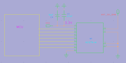
13. Apprication of 315/433/868/915 MHz RF Transceiver Module
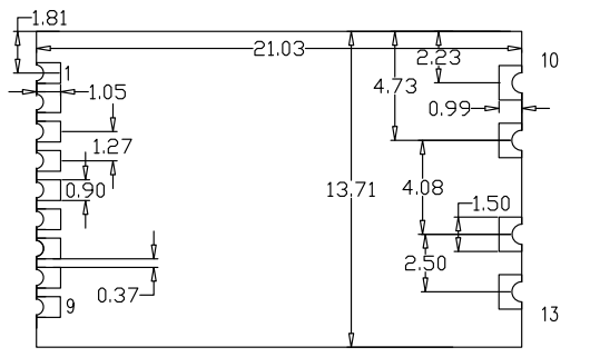
14. Module Package Outline Drawing of 315/433/868/915MHz RF Transceiver Module
Unit: mm
15. Ordering Information of 315/433/868/915 MHz RF Transceiver Module
Model | Part Number |
Operation Band |
RY1276 |
RY1276-315 |
315MHz |
RY1276 |
RY1276-433 |
433MHz |
RY1276 |
RY1276-868 |
868MHz |
RY1276 |
RY1276-915 |
915MHz |
16. Module Revisions of 315/433/868/915 MHz RF Transceiver Module
Revisions |
Date |
Updated History |
Rev1.0 |
March 2016 |
The first final release |
-
ASK Super Regeneration Receiver Module 5 Pieces / (Min. Order)
-
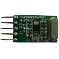
CATV FTTH Optical Receiver Module 5 Pieces / (Min. Order)
-
40 To 860MHz 20.6dB Gain CATV Module 5 Pieces / (Min. Order)
-
860MHz 20dB gain Hybrid amplifier module 5 Pieces / (Min. Order)

-
868.35MHZ RF Transmitter Module 1 Pieces / (Min. Order)
-
315MHZ ASK Transmitter Module 1 Pieces / (Min. Order)
-
433.92MHZ RF Transmitter Module 1 Pieces / (Min. Order)

-
433.92MHZ ASK Transmitter Module 1 Pieces / (Min. Order)
 Favorites

-
ASK Super Regeneration Receiver Module
5 Pieces / (Min. Order)
-
CATV FTTH Optical Receiver Module
5 Pieces / (Min. Order)
-
40 To 860MHz 20.6dB Gain CATV Module
5 Pieces / (Min. Order)
-
860MHz 20dB gain Hybrid amplifier module
5 Pieces / (Min. Order)
-
868.35MHZ RF Transmitter Module
1 Pieces / (Min. Order)
-
315MHZ ASK Transmitter Module
1 Pieces / (Min. Order)
-
433.92MHZ RF Transmitter Module
1 Pieces / (Min. Order)
-
433.92MHZ ASK Transmitter Module
1 Pieces / (Min. Order)